
The external clock in my TMO cell is becoming a dedicated board: USB control, oscillator, power supplies and level adaptation on one PCB. The reference remains adjustable from the Raspberry Pi, making the setup reproducible without dismantling an old SoftRock receiver.
From a working modification to a dedicated board
The existing Si570 modification runs at my station and has demonstrated reference-clock adjustment during operation. Board R1 combines the hardware and uses new firmware for an STM32 controller.
Status, 16 November 2026: Schematic, layout and firmware are prepared. Electrical rules and PCB checks report no errors; both firmware variants compile. The new board has not yet been manufactured or tested with an SXceiver. Results from the running SoftRock modification are therefore not measurements of this new hardware.
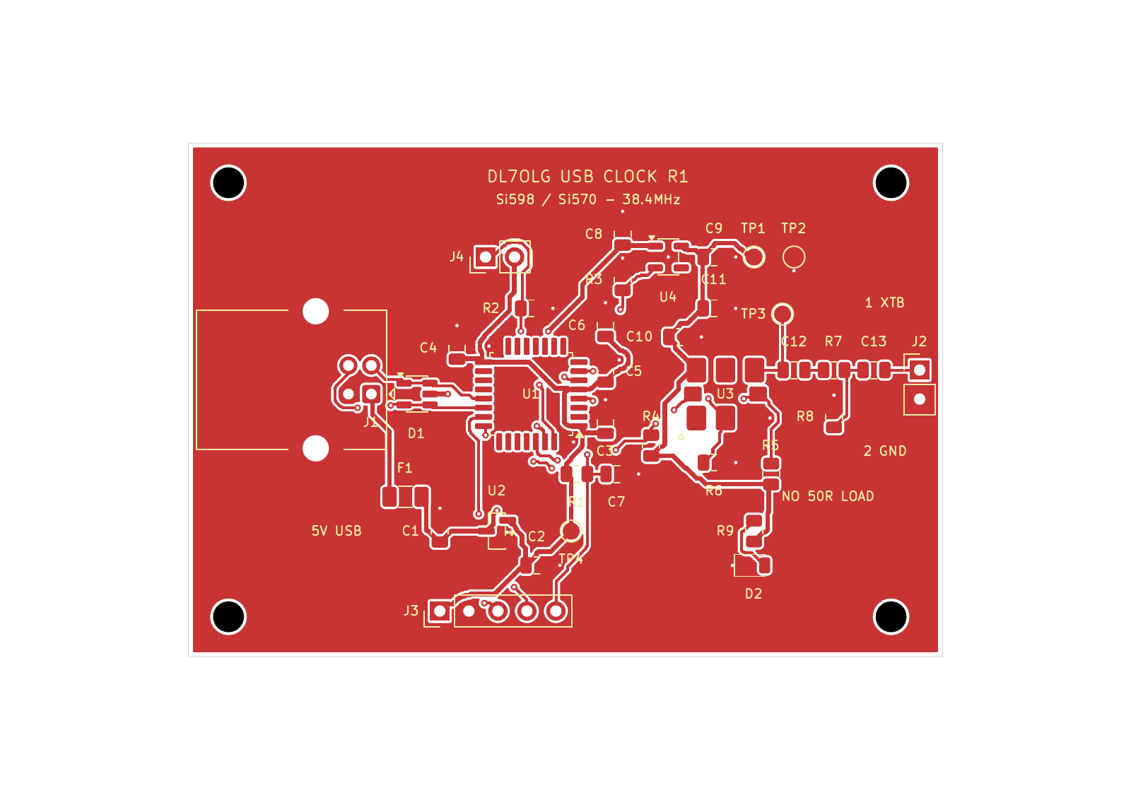
What is on the board?
- USB-B connector: Power and control through one cable, with input ESD protection and a resettable fuse.
- STM32F042K6T6: Native USB, dedicated control firmware and I²C to the oscillator. Firmware uses the TinyUSB stack.
- Separate 3.3 V supplies: One for the controller and a switched supply for the oscillator.
- Si598 or Si570: Specifically the 3.3 V CMOS parts 598PAC000141DG and 570CAC000141DG, each with a 56.320 MHz factory frequency. Firmware configures 38.4 MHz.
- Level adaptation and AC coupling: Output intended for the described modification at the SX1255 XTB clock input.
- SWD, boot jumper and test points: For programming, troubleshooting and board commissioning.
Si598 is the primary assembly option; Si570 is the alternative. Other parts in these families are not automatically interchangeable: output type, supply, OE polarity and factory frequency must match the circuit and firmware profile. The design uses the Skyworks Si598/99 datasheet.
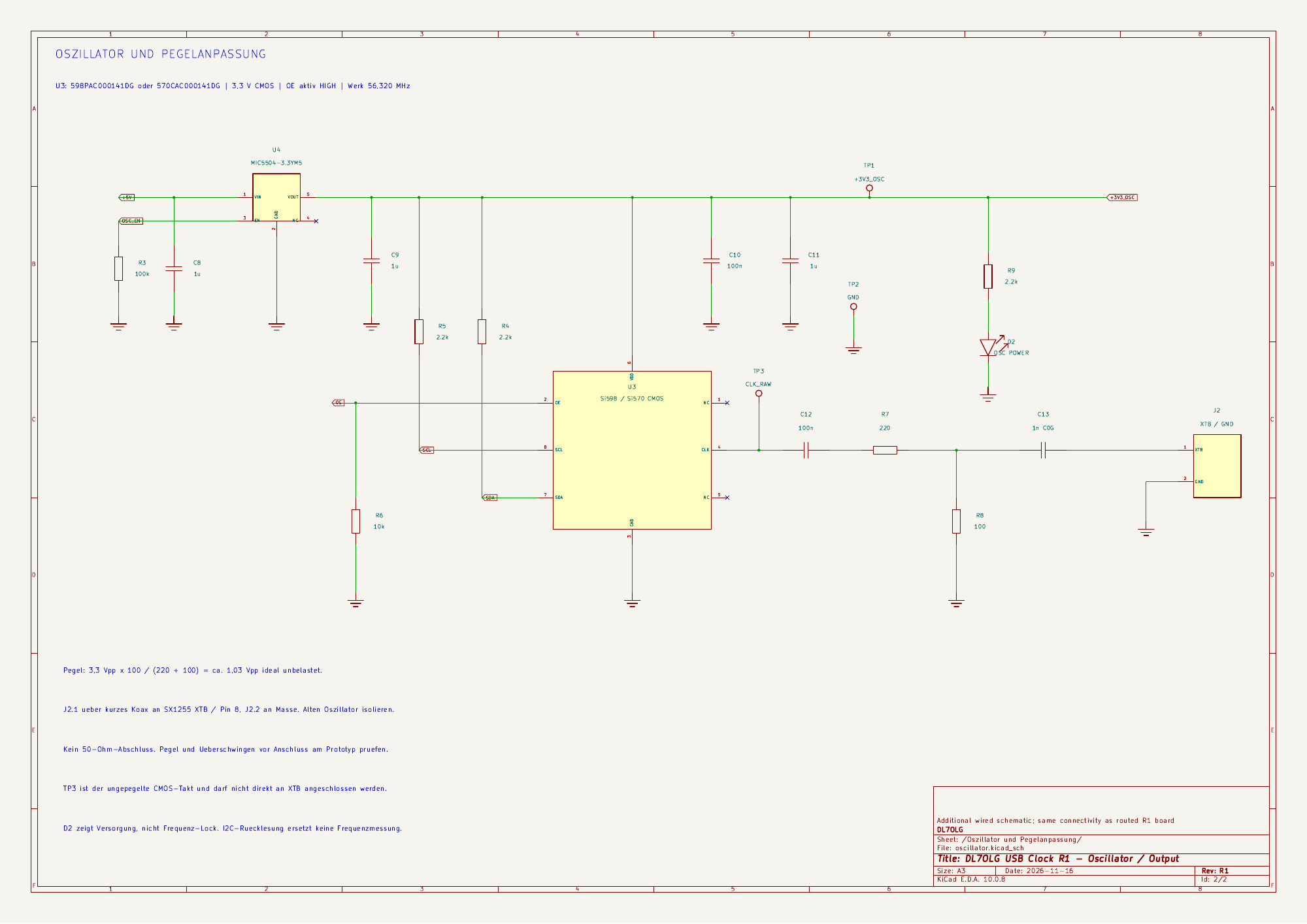
Drawn schematic with connecting wires
The schematic has two sheets. Sheet 1 contains USB, protection, controller, supply and programming connections. Sheet 2 contains the oscillator, its switched supply and complete level adaptation. Matching labels connect the sheets; ground is a shared net.
Top-side assembly drawing as PDF
Why level adaptation is necessary
The oscillator’s full CMOS output must not be connected directly to the reference input. A 100 nF coupling capacitor feeds a divider with 220 Ω in series and 100 Ω to ground. A subsequent 1 nF capacitor isolates the SX1255’s DC operating point from the divider.
Ideally, without loading, 3.3 V peak-to-peak becomes about 1.03 V peak-to-peak. The actual connected-board level, including overshoot, is what matters. J2 carries the adapted clock and ground; use a short shielded connection to XTB. Electrically disconnect the original oscillator first. Do not terminate this output with 50 Ω. Check the connection point individually on unknown SXceiver clones.
Dedicated firmware and USB programming
The new controller is independent of PE0FKO’s ATtiny firmware. At startup, output remains disabled while firmware recalls factory registers, calculates the setting and programs 38.4 MHz. Output is enabled only after successful readback. Small corrections use the prescribed Freeze-M sequence with unchanged dividers.
The USB descriptor requests 200 mA. The oscillator powers up only after USB configuration. A 500 mA USB 2.0 port provides enough capacity for the intended load. Actual current and behaviour during connection, disconnection and USB suspend remain part of prototype testing.
The STM32 includes a USB DFU bootloader, with SWD available too. Updating firmware interrupts the reference clock, so stop the cell first. Laboratory firmware uses an explicitly designated test identifier. A properly assigned USB identifier is required before distribution.
Working with software frequency control
I²C programs the oscillator and reads registers; it does not measure actual drift. Frequency estimation on the Pi uses the SXceiver’s running I²S sample counters and chrony’s corrected timebase.
In web interface 0.5.7, this is an optional Pro feature for the already tested USB Si570 setup. Once measurement quality is sufficient, its uncertainty-dependent control threshold allows corrections below 0.5 ppm. Disabling control leaves time synchronisation and measurement running.
The new board uses its own USB protocol. Integration into the existing web panel driver follows electrical commissioning. It is not yet a drop-in replacement for the current PE0FKO interface. Firmware reports a value calculated from programming; independent frequency measurement remains separate.
Next checks
Digital checks cover connectivity, track clearances, register calculations and firmware error handling. Before RF operation, the assembled board needs USB enumeration and current measurements, output-level and edge checks, actual-frequency measurement and testing of small clock corrections. A schematic and chrony display alone establish neither jitter nor guaranteed absolute frequency accuracy.
The running modification and observations are documented in the SXceiver Si570 article. This new project documents development of the standalone USB board.
Download CAD and manufacturing files
For PCBWay or another PCB manufacturer: The Gerber ZIP includes copper, solder mask, silkscreen, outline, paste and separate plated/non-plated drill files. Upload it as the PCB manufacturing dataset.
- PCBWay Gerber package R1 · ZIP · 72 KiB · SHA-256
- Complete KiCad package R1 · ZIP · 3.5 MiB · SHA-256
The complete package contains editable KiCad PCB and both schematic versions with libraries, PDF drawings, Si598/Si570 bills of materials, placement coordinates, firmware sources and validation reports.
PCB specification: 66 × 45 mm, two layers, FR4, 1.6 mm thick, 35 µm copper (1 oz). Further specifications are in manufacturing/PCBWay/README.txt. For assembly, also supply the matching BOM and placement file from the complete package. Do not mix oscillator variants.
R1 is an unbuilt development revision. Digital checks are complete; current, output levels and SXceiver operation need prototype verification. Firmware uses a test USB identifier and is not yet cleared for production distribution.